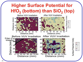

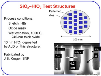
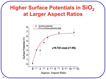
High-k Dielectric Patterned
During plasma-processing steps charging of the patterned dielectrics can take place notably by ion shading effect. We measure photoemission yield during radiation exposure and surface potential measurements of the samples to correlate charging of the patterned dielectrics to the aspect ratio of the features. Our work is focused on Hafnium Oxide and Silicon Dioxide patterns.
|
|
|